PCI Express in short called PCIe is a high speed serial interconnect. PCIe is used in processor based designs. PCIe helps to interface processor with Graphics cards, network adaptors (for Ethernet), Wireless adaptor Cards like that of Wi-Fi, Ethernet Switches, PHY chipsets, etc., PCIe interface has something called lanes for transmitting data between the processor and the devices. A lane is a differential Tx and Rx lines . PCIe standard has lanes starting from x1 till x16.
PCIe has evolves over the period of time and has several versions. For examples, PCIe Version 1.0a has 1 lane (x1) and 16 lanes (x16) option with a maximum bit rate of 2.5 GT/s. and high band-width version of PCIe which is version 7.0 has a maximum bit rate of 128 GT/s.
PCIe is a point-to-point serial interconnect interface. This meant two devices are connected one to one using lanes. The terminology used for connection between PCIe devices is “interconnect” or “link”. There is confusion among engineers understanding the difference between link and lane. A link refers to the complete PCIe interface between the PCIe devices where as a lane refers to the Tx and Rx differential pair. A link can have multiple lanes.
PCIe topology is as below:
As we can see from the above topology, CPU interfaces with PCIe devices using the Root Complex. Root Complex has PCIe interface and helps processor by taking care of the interface. Root complex able to see all end point in system. The two major terminologies used in PCIe are Host and Endpoint. In the above architecture, CPU is the host and devices connected to CPU are called the end-points. We can see that the multiple end points can be connected to a single PCIe interface using the PCIe switch. This looks like creating multiple end-points from a single end-point. While this kind of approach seems like limiting the PCIe band-width, the switch has mechanism to ensure that band-width is not limited.
.
PCIe lanes carry data packets between the host and the end point. When x1 lane is used, packet is transmitted entirely over that line. If there is more than x1 lane, then the data packet is distributed across these lanes which help in faster data transmission. This is kind of parallel transmission over serial differential lanes.
In PCIe device which can initiate a data request is called an end point. Each Endpoint is identified by a requester ID.
Below is a list of standard lane count in a PCIe interface:
• x1 lane
• x2 lanes
• x4 lanes
• x8 lanes
• x16 lanes
Below image shows PCIe slots on a Mother board:
We can see from the above image that the PCIe slots are included on the board to plug-in PCIe cards. The below images shows an example of PCIe add-on card which can be plugged into the PCIe slot. We can see that there is edge finger connection on this card which helps the card to plug-in into the PCIe slot. These edge connections are commonly gold connections as they provide superior conductivity.
The above pin out defines the x1 connectivity, where there is only single lane.
- HSOp/n and HSIp/n are transmit and receive lanes respectively.
- Reference clock is supplied such that a single clock domain can be maintained and the end point can derive a higher clock from this reference clock.
- PRSNT#1 must be tied to PRSNT#2
- WAKE# and PERST# are open-drain signals
PCIe x1 Power requirements
As seen in the above x1 pin out, there are +12V and +3.3V power pins. So, the host card has to supply power to the PCIe add-on card and for different connector types (x1, x4, x8, x16) power requirements vary. For a x1 connector, 12V must be able to supply 500mA and 3.3V must be able to supply 3A. There is 3.3Aux rail as well which must supply 375mA of current. The power requirements shall be more for the x4, x8, x16 boards
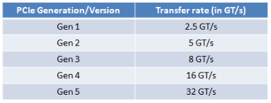
PCIe Transfer Rates
The below table shows the PCIe transfer rates in various generations:
The above transfer rates in the table are for a single lane. If x2 is used, transfer rate becomes x2. Gen 5 support processors are available in the market. Intel chip set Alder Lake which is a Intel 12th Generation chip set supports PCIe Gen5.
Upstream and Downstream
When talking about the PCIe interface, we always use the terminologies upstream port and downstream port. An Upstream Port is a port that points in the direction of the CPU/root complex. A Downstream Port is a port that points away from the CPU/root complex
Advantages of PCIe:
• Low Pin count unlike the PCI with parallel signals
• PCIe provides a scalable option with multiple lanes option
• PCIe card with smaller lane size like for example x1 can fit into a x4 slot. This ensures that x4 and x1 can be used with the same slot.
• High Throughput
• Hot-swap option
• AER (Advanced Error Reporting)
• No External clock for as clock is recovered from the data
• As clock is not present, no problem with Data skew
Acronyms:
• PCIe = Peripheral component interconnect Express
• Tx = Transmit
• Rx = Receive
• GT/s = Giga Transfers/Second


 ]]>
]]>


0 Comments