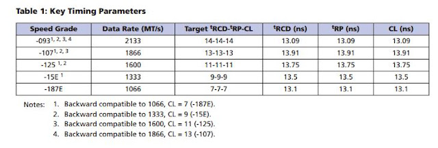
Understanding the specifications from the DDR datasheet is crucial to a successful design. Whether it be DDR or any electronics device, the successful design without many revisions can happen only if designer can understand the datasheet specifications thoroughly. Let us take MT41J256M4 from Micron for detailed understanding of the specifications. MT41J256M4 is a DDR3 SDRAM memory.
Data Rate:
The data rate specification here talks about the rate at which the data can transferred to and from DDR. The specification here talks in terms of MT/s which means one million (10^6) transfers per second. As the DDR is dual data rate operating memory, if the data rate of 2133 MT/s is taken, the clock frequency would be half of it which comes to 1066 MHz. For any designer who is going to pick the DDR memory, one of the crucial steps would be to check out the DDR type and data rate supported by the processor.
For any DDR, the maximum data rate that can be achieved is,
Clock frequency * (Number of bits of data/8)
Here, number of bits is indicator to the data lines of the DDR memory.
tRCD-tRP-CL:
The tRCD-tRP-CL are more of RAM timing parameters. You see values like 14-14-14, 13-13-13, etc. These values are an indicative to the performance of the DDR. These are mainly related to the internal data accessing of the RAM. So, coming back to the main point, what does 14-14-14 mean is that they indicate the number of clock cycles. In the above table, you could see the value of tRCD given as 13.09ns. So, for a 2133MT/s DDR which operates at 1066MHz rate, if you consider the ratings given of tRCD as 14, you get ((1/1066M) * 14), which comes to 13.09ns. The important thing to notice in this timing parameters is that as the clock frequency is reduced the accessing of RAM is much faster.
One thing to remember here is that the timings we are discussing here are independent of the clock frequency of the DDR memory.
tRCD - Row address to Column address delay
The delay between (or clock cycles required) activating a row inside a DDR and accessing the columns. this is also called RAS to CAS delay.
When we talk about the architecture of RAM, we see terms like banks, rows, columns. The size of the column inside a DDR will be of data bus width size. For example, if you have a 8-bit DDR data bus, each column would be 8-bit. So, column is smallest addressable unit inside a DDR. There will be arrays of columns for each row. These rows are part of banks. There are bank select pins for a DDR to select particular bank. And the address pins to access particular location. In addition, DDR has RAS and CAS pins to differentiate between row and column address.
CL - Column Latency
The delay between the time for which column address is sent to the DDR and the first bit is received in response. In general terms, it is more of a delay between query and response. The query to DDR will always be a address (either read or write cycle) and DDR in turn returns data.
tRP - Row pre-charge time
If we are accessing a row inside a DDR already and wanted to access a new row, the time taken for disabling present row that is accessed and selecting another row for access. Precharge is basically a command used to close a bank that is activated.
RAS - Row address strobe
CAS - Column address strobe


2 Comments
good article to understand basics.
ReplyDeleteGood article.. thank you
ReplyDelete