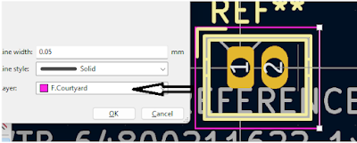
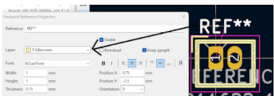
In this post, we will list the sections of a PCB Footprint for a particular component.
Courtyard:
In PCB design, the term "component courtyard" refers to the minimum clear space required around a component on the PCB. This clear space ensures that there is no interference between the component and other components, traces, or the board edge. The component courtyard helps prevent electrical shorts, ensures proper heat dissipation, and allows for easier assembly and maintenance of the PCB.
Silk Screen:
Each component has a reference designation on the board which is part of the silk screen of the board. Apart from reference designation, the silk screen contains markings, symbols, and text to indicate component placement, orientation, and other important information for assembly and servicing. It is typically white in color and is printed on the top and/or bottom of the PCB, providing a visual guide for placing components and soldering them onto the board. The silk screen helps ensure that components are placed correctly and that the board is assembled according to the design specifications.
Solder Paste:
Solder paste is a mixture of small solder spheres suspended in a flux medium. It is used in the assembly of printed circuit boards (PCB) to facilitate the soldering of surface mount components (SMD) onto the board.
During the PCB assembly process, solder paste is applied to the pads on the PCB using a stencil. The components are then placed onto the solder paste, and the entire assembly is heated in a reflow oven. The heat melts the solder paste, which then solidifies to form a permanent electrical and mechanical connection between the components and the PCB.
Solder paste is essential for SMD assembly because it allows for precise application of solder to the pads, ensuring good electrical contact and strong mechanical bonds. The flux in the solder paste also helps to remove oxidation from the surfaces being soldered, improving the quality of the solder joint.


0 Comments